The Quantum Information and Technologies team is hiring a highly motivated postdoctoral researcher to work in the exciting field of nonlinear integrated quantum photonics. The successful candidate will work in a highly collaborative research environment, have access to state-of-the-art facilities for device fabrication and characterization, and will contribute to the development of novel optoelectronic devices with applications in quantum technologies.
The team is at the international forefront in the development of semiconductor devices for the generation and manipulation of quantum states of light, exploiting both discrete and continuous degrees of freedom of light. The exploited material, AlGaAs, presents several assets in the landscape of platforms for integrated quantum photonics, which have been exploited to reach several key results: direct bandgap allowing for the monolithic integration of pump laser and internal SPDC [1], mature fabrication techniques for the development of quantum photonic circuits [2,3], high second-order nonlinearity leading to high pair generation rates [4], high versatility in the engineering of the biphoton state [5,6,7], utilization of the devices in quantum information protocols [8].
The postdoc project aims to push further the functionalities of the devices in terms of electrical injection in both monolithic and hybrid (AlGaAs/SOI) devices, exploitation of the Electro-Optics effect for quantum state manipulation in simple waveguides or more complex quantum photonic circuits, opening the door to exciting applications in quantum communication, computing, and metrology.
Responsibilities:
* Design, fabricate, and test integrated semiconductor photonic devices
* Develop theoretical models and simulations to predict the performance of integrated photonic devices
* Work with Ph.D. students and other members of the group and with external collaborators for the devices’ characterization in the quantum regime and their utilization in quantum information protocols
* Actively participate in the publication of research results in high-quality scientific journals and their presentation at national and international conferences
Qualifications:
* Ph.D. in physics
* Strong background in photonics and optoelectronics
* Experience in the design and characterization of integrated photonic devices
* Knowledge of semiconductor optoelectronic device physics and their fabrication process is highly desirable
* Experience with simulation software, such as Lumerical or COMSOL
* Ability to work effectively in a team
The position is available starting from the beginning of 2024, and the initial appointment is for one year, renewable. The salary is based on French regulations and depends on the candidate’s previous experience.
Interested candidates may contact Sara DUCCI (sara.ducci@u-paris.fr) as soon as possible. The application should contain a CV, a list of publications, a short research statement (cover letter), and contact information for two senior researchers who can provide recommendation letters.
[1] F. Boitier et al. Phys. Rev. Lett. 112, 183901 (2014)
[2] J. Belhassen et al. Appl. Phys. Lett. 112, 071105 (2018)
[3] F. Appas et al. ACS Photonics 10, 1136 (2023)
[4] F. Appas et al. IEEE J. of Lightwave Technology (invited paper) 40, 7658 (2022)
[5] S. Francesconi et al. Optica 7, 316 (2020)
[6] S. Francesconi et al. ACS Photonics 8, 2764 (2021)
[7] S. Francesconi et al. Photonics Research 11, 270 (2023)
[8] F. Appas et al. Nature Partner Journal Quantum Information 7,118 (2021)
À lire aussi

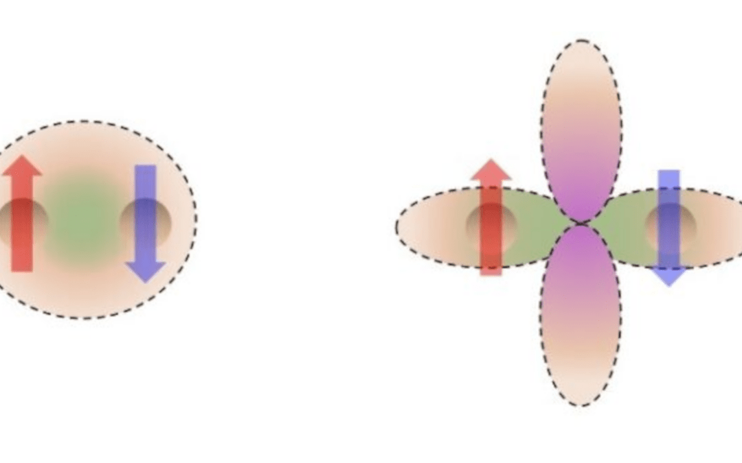
Manipulating unconventional superconducting states via anisotropic strain
Laboratoire: MPQ (Matériaux et Phénomènes Quantiques), Université Paris Cité & CNRSAdress: Bâtiment Condorcet – 10 Rue A. Domon et L. Duquet – 75013 ParisInternship/PhD supervisor: Yann GallaisTel: 0157276989e-mail: yann.gallais@u-paris.fr Scientific project:...

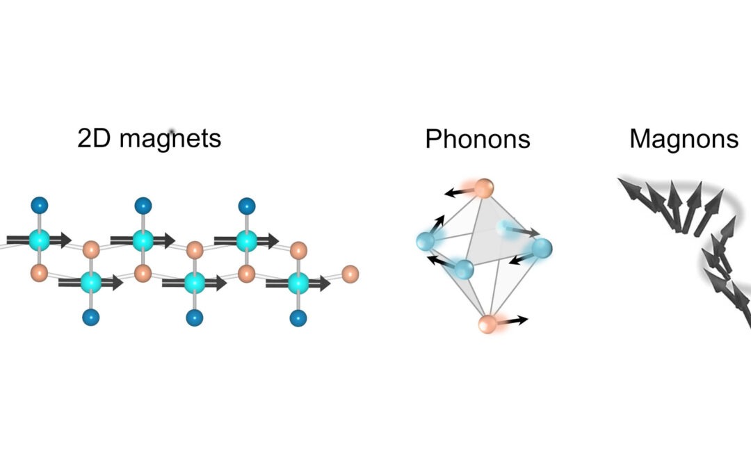
Towards light control of van der Waals magnets
Laboratoire: MPQ (Matériaux et Phénomènes Quantiques), Université Paris Cité & CNRS Adress: Bâtiment Condorcet – 10 Rue A. Domon et L. Duquet – 75013 Paris Internship/PhD supervisor: Niloufar Nilforoushan and Yann Gallais Tel: 0157276223 e-mail:...

Exploring Exotic Electronic States in 2D Transition Metal Dichalcogenides
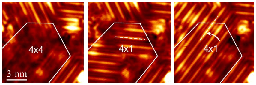
Figure 1: Successive STM images of VTe2 monolayer where CDWs are manipulated by local excitation. From left to right, a 4x4 phase is switched to 4x1 and the 4x1 phase is rotated [1]. Laboratoire: MPQ (Matériaux et Phénomènes Quantiques), Université Paris Cité &...

Propriétés électroniques des allotropes de phosphorène contraints
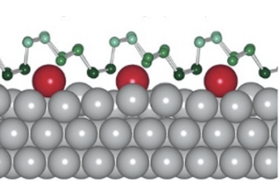
(a) Schéma d'une surface vicinale. (b) Un des allotropes du phosphorène. (c) Résolution atomique par STM. Laboratoire: MPQ (Matériaux et Phénomènes Quantiques), Université Paris Cité & CNRSAdresse: Bâtiment Condorcet – 10 Rue A. Domon et L. Duquet – 75013...
