
Laboratoire: MPQ (Matériaux et Phénomènes Quantiques), Université Paris Cité & CNRS
Adress: Bâtiment Condorcet – 10 Rue A. Domon et L. Duquet – 75013 Paris
Internship/PhD supervisor: Yann Gallais
Tel: 0157276989
e-mail: yann.gallais@u-paris.fr
Scientific project:
Transition metal dichalcogenides (TMDs) have recently attracted significant interest because they allow the exploration of novel quantum phenomena down to the 2D limit. Of particular interest for the present project are metallic TMD like NbSe2 which displays various quantum phases like Superconductivity (SC) and charge density wave (CDW) states. In addition, the possibility of creating Van der Waals heterostructures (VdW) by vertically stacking 2D materials provide a fertile playground to engineer novel properties and devices. Of particular interest are the Moiré patterns due to the lattice mismatch and crystalline misalignment between vertically stacked layers. Indeed, quantum interference effects between sheets of the 2D TMD with a twist angle allows an unprecedented control of the effective electron kinetic energy scale, driving the system to an interaction dominated regime and drastically enhancing anisotropies, thus providing a pathway to engineer SC properties at the 2D scale.
During the internship, the student will initiate the fabrication of TMD-based VdW heterostructures displaying SC properties using exfoliation techniques. Samples of NbSe2 will be fabricated and characterized as a function of thickness and twist angle. The obtained samples will be first measured by transport measurements to assess their presence of SC and its critical temperature. Going beyond traditional transport measurements, an originality of the project will be the use of low temperature spectroscopic techniques with micron-size spatial resolution like Raman scattering to probe the SC state.
Contact: Yann Gallais
À lire aussi

Exploring Exotic Electronic States in 2D Transition Metal Dichalcogenides
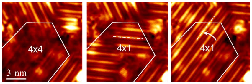
Figure 1: Successive STM images of VTe2 monolayer where CDWs are manipulated by local excitation. From left to right, a 4x4 phase is switched to 4x1 and the 4x1 phase is rotated [1]. Laboratoire: MPQ (Matériaux et Phénomènes Quantiques), Université Paris Cité &...

Propriétés électroniques des allotropes de phosphorène contraints
(a) Schéma d'une surface vicinale. (b) Un des allotropes du phosphorène. (c) Résolution atomique par STM. Laboratoire: MPQ (Matériaux et Phénomènes Quantiques), Université Paris Cité & CNRSAdresse: Bâtiment Condorcet – 10 Rue A. Domon et L. Duquet – 75013...

Controlling the properties of 2D materials at the atomic scale by defect engineering
Laboratoire: MPQ (Matériaux et Phénomènes Quantiques), Université Paris Cité / CNRSAdress: Bâtiment Condorcet – 10 Rue A. Domon et L. Duquet – 75013 ParisInternship/PhD supervisor: Jérôme LagouteTel: 0157276299e-mail: jerome.lagoute@u-paris.fr STM image (20 nm x 40...

Quantum interference of spin currents in hybrid 2D materials/molecules interfaces
Laboratoire: MPQ (Matériaux et Phénomènes Quantiques), Université Paris Cité & CNRSAdresse: Bâtiment Condorcet – 10 Rue A. Domon et L. Duquet – 75013 ParisDirecteur de stage/thèse: Clément BarraudTel: 0627065271e-mail: clement.barraud@u-paris.fr Scientific...
