

Research topics
The team is developing several research activities around surface physics.
Spin-crossover molecules on surfaces
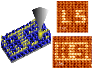
Left) Illustration of voltage pulse manipulation. Right) Topographic STM images (V=0.3 V, I=3 pA) of 10x10nm2 (top) and 10×12.5nm2 (bottom) on which “LS” and “HS” have been written by voltage pulse manipulation
Spin-crossover molecules are organometallic complexes exhibiting two spin states – high spin (HS) and low spin (LS) – that can be controlled by external stimuli such as temperature, light or voltage. These switching properties, along with the bistability and reversibility of the transitions, make spin-crossover molecules promising candidates for incorporation into controllable electronic or spintronic devices. Developing robust devices requires a thorough understanding of molecule-substrate interface properties. Consequently, the central question, driving the team’s research, is how spin-crossover molecules retain their properties upon adsorption onto various types of substrates (metals, ferromagnets, graphene). To this end, we focus on model systems created by the sublimation of molecules under ultra-high vacuum conditions, yielding molecular films with thicknesses ranging from sub-monolayer to several tens of monolayers. The structure and transition properties of these molecular films are then determined using complementary techniques at the nanoscale via scanning probe microscopy measurements (STM/STS and AFM), and at the micrometer scale via x-ray absorption spectroscopy (XAS) and grazing-incidence X-ray diffraction (GIXD) measurements realized on synchrotron facilities.
Scientific collaborators: Talal Mallah and Marie-Laure Boillot (ICMMO, Université Paris Saclay / CNRS), Marie-Anne Arrio (IMPMC, Sorbonne Université / CNRS), Edwige Otero (ligne DEIMOS, synchrotron SOLEIL), Alessandro Coati (ligne SixS, synchrotron SOLEIL), Cyrille Barreteau and Alexander Smogunov (SPEC, CEA Saclay), Yannick J. Dappe (C2N, Université Paris Saclay / CNRS), Shobhana Narasimhan (Jawaharlal Nehru Centre for Advanced Scientific Research, Inde)
Chirality at interfaces
The surface structure, especially of low-symmetry surfaces and interfaces, is important from both fundamental and applied points of view, as its behavior differs significantly from that of the bulk of a material.
Chiral objects, which lack any improper symmetry element, can exist in two non-superimposable forms. Chirality has been found to give rise to exotic emergent properties in fields like electronics, chemistry, optics, magnetism, and spintronics, with such properties depending on the exact chiral form.
Various chiral systems are being investigated in the group, using scanning probe microscopy techniques like scanning tunneling microscopy and atomic force microscopy, and diffraction methods such as X-ray diffraction and grazing incidence X-ray diffraction. This range of techniques allows for the study of both chiral surfaces and interfaces of different inorganic materials and hybrid systems consisting of molecules on surfaces.
Scientific collaborators : Pascal Martin and Sophie Nowak (ITODYS, Université Paris Cité / CNRS), Alessandro Coati (beamline SixS, synchrotron SOLEIL)
Charge density waves in 2D materials
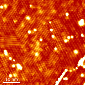
STM image of a VTe2 monolayer on graphene showing multiple domains of various charge density waves. [U. Chazarin et al., Nano Letters 24, 3470 (2024)]
Charge density waves (CDWs) are collective electronic states resulting from the coupling between electrons and the atomic lattice of materials. In transition metal dichalcogenides (TMDs), they provide an ideal framework for studying emerging electronic phases in quantum materials and their control.
The team conducts research on CDWs in two-dimensional TMDs, investigating them experimentally using scanning tunneling microscopy and spectroscopy (STM/STS). Our goal is to understand the fundamental mechanisms governing the formation and dynamics of charge density waves, as well as to explore their modulation and control in order to engineer new functionalities in two-dimensional materials.
U. Chazarin et al., Nano Letters 24, 3470 (2024)
U. Chazarin et al., Adv. Mater. Interfaces 10, 2201680 (2023)
2D Phosphorus
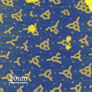
STM image of Hexagonal Phosphorus nanostructures grown on Au(111). [A. Karn et al. Small 2405924 (2024)]
The quest for novel two-dimensional (2D) materials with exotic electronic properties holds great promise for next-generation electronics. Among these, phosphorene—alongside its bulk counterpart, black phosphorus (BP)—has garnered particular interest due to its remarkable structural, electronic, and optical properties. Unlike graphene, phosphorene’s non-planar structure enables the existence of numerous allotropes, offering a rich diversity of structural and electronic configurations.
Our team focuses on the study of new phosphorene allotropes and nanostructures, exploring their growth under UHV on metallic substrates and atomic-scale electronic properties. The latter are characterized using scanning tunneling microscopy and spectroscopy (STM/STS). We also analyze how interactions with the substrate influence their growth modes and modulate their electronic properties.
A. Karn et al. Small 2405924 (2024)
R. Harsh et al., J. Phys. Chem. Lett. 13, 6276{6282 (2022)
Defect engineering

STM image of a p-n type junction in nitrogen-doped graphene, showing a 7 nm-wide transition region. [M. Bouatou et al., Adv. Funct. Mater. 32, 2208048 (2022)]
A major challenge in 2D materials research is to go beyond their intrinsic properties by engineering them in a controlled manner. A particularly promising strategy involves the use of atomic defects as a novel tool for materials engineering.
Our team is exploring this approach by creating controlled defects to achieve new functionalities in 2D materials. These defects are characterized using scanning tunneling microscopy and spectroscopy (STM/STS), allowing to probe their structure and electronic properties at the atomic scale. Nitrogen doping of graphene is an example of such strategy: by replacing some carbon atoms by nitrogen the electronic structure is modified, allowing to achieve band engineering or new chemical and catalytic properties. Other defects in various materials are being investigated to achieve new functionalities useful for applications such as nanoelectronics and catalysis.
D. Demba et al., ChemPhysChem e202400221 (2024)
M. Bouatou et al., Adv. Funct. Mater. 32, 2208048 (2022)
M. Bouatou et al., Nano Letters 20, 6908 (2020)
R. Harsh et al., J. Phys. Chem. Lett. 6897 (2019)
F. Joucken et al., Phys. Rev. Mater. 3, 110301 (2019)
Surfaces' structure
Item 1
Légende
Details coming soon
À lire aussi

Florent Baboux elected IUF Junior Member
Florent Baboux, associate professor at MPQ laboratory, has been elected a Junior Member of the Institut Universitaire de France (IUF) under the Fundamental chair. Congratulations! His research aims to use light to explore and control quantum phenomena that remain...
The sky of quantum light is not flat
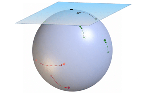
In a recent study, researchers from the QITE team at MPQ and from the department of Mathematics of ENS have refined the mathematical framework needed to coherently describe quantum states involving multiple photons. (Left) When the phase reference is explicitly...
An optomechanical disk in its fundamental state of motion
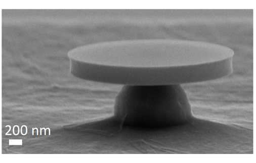
The motion of a mesoscopic mechanical resonator can exhibit quantum behavior when cooled to very low temperatures. In particular, it can reach its ground state and cease to vibrate. Using light as a probe, the LIME team at the MPQ laboratory demonstrated that...
Watching gold switch between order and disorder
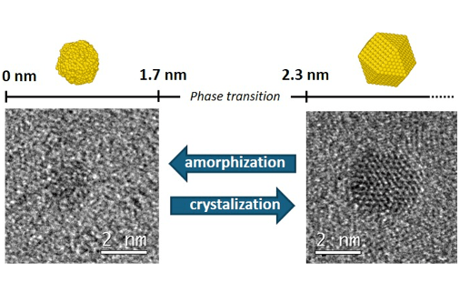
Researchers from Matériaux et Phénomènes Quantiques laboratory have directly observed, for the first time, a reversible phase transition between amorphous and crystalline states in ultra-small gold nanoparticles. Their findings reveal that the atomic structure of gold...