
Graphene, composed of a single layer of carbon atoms, possesses unique and promising physical properties in various fields, particularly in electronics.

Figure :
Diagram (left) representing a cluster of C60 molecules used as a mask to protect graphene during doping by exposure to nitrogen activated by a plasma source. 3D STM image (right, top) showing a junction in graphene with low doping on the left and high doping on the right. Each bump in the image corresponds to a nitrogen atom substituted for carbon. The colors corresponding to local conductance indicate the doping evolution along the junction (low in yellow, high in blue). The doping profile (Dirac point energy of graphene) along the junction allows for measuring the width of the transition zone, which is 6.6 nanometers in this example (bottom right).
The elementary building block of electronic components is the p-n junction, which involves bringing together two regions of a material with different doping levels. An important parameter in these junctions is the width of the transition zone at the interface. In graphene, when this width is ultra-thin (less than 20 nanometers), electron-optical phenomena, such as electron collimation, can occur. The atomic-scale properties of junctions in chemically doped graphene, analogous to p-n junctions in semiconductors, have remained unexplored until now.
Physicists from the Materials and Quantum Phenomena Laboratory (MPQ, CNRS/Université Paris Cité) and the Condensed Matter Physics Service (SPEC, CNRS/CEA/Université Paris Saclay), in collaboration with the Technical University of Denmark (DTU), have developed a method to create junctions in nitrogen-doped graphene and visualize and measure their electronic properties at the atomic scale. To nanostructure nitrogen, islands consisting of a single layer of C60 molecules were used as masks during the exposure of graphene to nitrogen atoms activated by a plasma source. After removing the C60 through heating, the resulting sample exhibits lightly doped regions in the middle of more heavily doped regions, with the interface between the two forming a p-n junction within the graphene plane. By using a scanning tunneling microscope (STM), these junctions could be visualized with atomic resolution. Locally performed spectroscopic measurements allowed for measuring the doping profile along the junction as well as the width of the transition zone. This width corresponds to the two-dimensional equivalent of the space charge region in p-n junctions based on traditional semiconductors. This width appears to be around 7 nanometers, which is well below what has been achieved previously in field-effect devices. These results are supported by electronic structure calculations within the framework of Density Functional Theory (DFT). In particular, these calculations show the spatial evolution of the Dirac point energy in graphene, which is synonymous with doping in this material. This evolution is specifically linked to the propagation of electron density from the nitrogen atoms into the graphene.
These findings represent the first atomic-scale visualization of junctions in doped graphene and open up several perspectives. On one hand, this result reveals the intrinsic width of p-n junctions in doped graphene and enables the realization of structures utilizing electron-optical effects. In this sense, these ultra-thin p-n junctions can be used to focus or guide electrons. On the other hand, the molecular monolayer mask method opens up the possibility of studying the effect of surface functionalization by various elements other than nitrogen on different materials by comparing functionalized and non-functionalized regions, which can be simultaneously measured with atomic-scale resolution.
This publication has been selected as a news item on the INP website.
Contact:
Jérôme Lagoute (jerome.lagoute@u-paris.fr)
Yannick Dappe (yannick.dappe@cea.fr)
Reference:
Visualizing in-plane junctions in nitrogen-doped graphene, M. Bouatou, C. Chacon, A. Bach Lorentzen, H. T. Ngo, Y. Girard, V. Repain, A. Bellec, S. Rousset, M. Brandbyge, Y. J. Dappe, J. Lagoute, Advanced Functional Materials 2208048 (2022)
À lire aussi
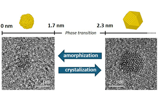
Watching gold switch between order and disorder
Researchers from Matériaux et Phénomènes Quantiques laboratory have directly observed, for the first time, a reversible phase transition between amorphous and crystalline states in ultra-small gold nanoparticles. Their findings reveal that the atomic structure of gold...
Exact low-energy duality in superconducting quantum circuits
The THEORIE team, in collaboration with Michel H. Devoret, has published a theoretical study in Physical Review Letters demonstrating an exact low-energy duality in circuits where a Josephson junction is coupled to a multi-mode environment. These systems exhibit a...
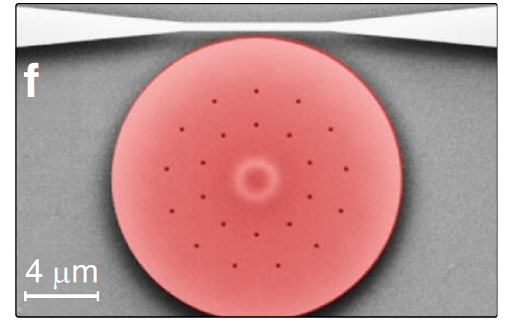
Multiphysics optomechanical sensing of a liquid on the micron scale
The LIME team at MPQ laboratory, in collaboration with CEA LETI in Grenoble, has published an article in Microsystems & Nanoengineering presenting an optomechanical platform for characterizing the rheological, optical, and thermal properties of fluids at the...
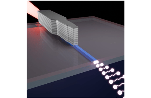
Biphoton state generation and engineering with bright hybrid III–V/silicon photonic devices
The QITE team at the MPQ Laboratory, in collaboration with STMicroelectronics, C2N, and INPHYNI, published a paper in Optica Quantum on the generation and engineering of two-photon states using III-V/SOI hybrid devices. Artist’s sketch of...