
Le laboratoire Matériaux et Phénomènes Quantiques (MPQ) est une Unité Mixte de Recherche (UMR 7162) du Centre National de la Recherche Scientifique (CNRS) et de l’Université Paris Cité.
Actualités
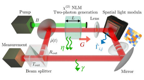
Equilibre émergent dans les machines d’Ising tout-optiques à trajectoires quantiques uniques
Une collaboration entre l’équipe Théorie de MPQ, le CREF de Rome et l’Université La Sapienza a montré que des systèmes optiques multimodes, excités par des processus à deux photons, peuvent atteindre un équilibre thermique au niveau des trajectoires quantiques...
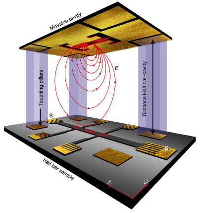
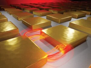
Cavity-enhanced fractional quantum Hall phases and cavity-modified spin splittings
Une collaboration entre l’Équipe Théorie de MPQ, l’ETH Zurich et le Flatiron Institute a démontré, à la fois théoriquement et expérimentalement, que les champs du vide géants confinés dans une cavité peuvent profondément modifier les interactions électron-électron...
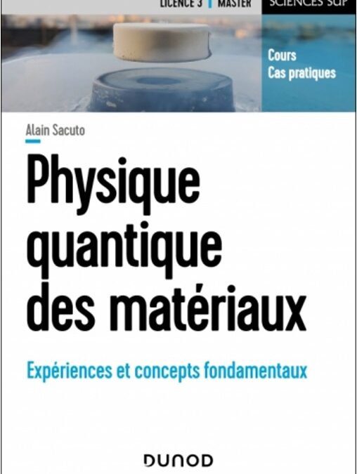
Parution du livre “Physique quantique des matériaux ” par Alain Sacuto
Alain Sacuto (équipe SQUAP) publie aux éditions Dunod son livre sur la Physique quantique des matériaux, fruit de nombreuses années d’enseignement à l’Université Paris Cité. La physique quantique des matériaux est au cœur des développements technologiques les plus...
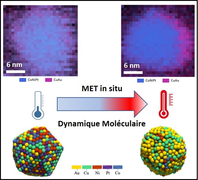
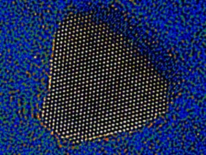
Stabilité thermique des nanoalliages à haute entropie : réalité ou chimère ?
En étudiant à l’échelle atomique le comportement thermique de nanoparticules composées d’or, de cobalt, de cuivre, de nickel et de platine, des scientifiques ont révélé que la stabilité de ces nanoalliages dits à haute entropie est beaucoup plus faible qu’espérée, car...
 Dispositifs Optiques Nonlinéaires (DON)
 Quantum Information and Technologies (QITE)
 Equipe THEORIE
 Lumière et Mécanique (LIME)
 Microscopie Electronique Avancée et Nano-Structures (MEANS)
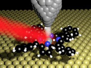 Auto-organisation de nanostructures et STM
 Spectroscopie de QUAsi-Particules (SQUAP)
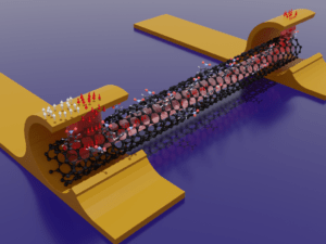 Transport Electronique à L’Echelle Moléculaire (TELEM)
Tutelles
