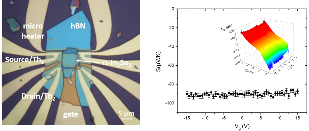
LEFT) Optical microscope image of a device based on α-In2Se3 . RIGHT) Measured Seebeck coefficient of α-In2Se3 as a function of the gate voltage. Inset: current-voltage characteristics of the device for different values of the gate voltage.
Laboratoire: MPQ (Matériaux et Phénomènes Quantiques), Université Paris Cité & CNRS
Adresse: Bâtiment Condorcet – 10 Rue A. Domon et L. Duquet – 75013 Paris
Directeur de stage/thèse: Maria Luisa Della Rocca
Tel: 0157277013
e-mail: maria-luisa.della-rocca@u-paris.fr
Scientific project:
Recently bidimensional (2D) van der Waals (vdW) III−VI semiconductors have drawn intense attention due to their unique electronic properties [1]. Among these materials, In2Se3 in its most studied a and b phases, shows a great potential for a wide variety of applications in electronics, photonics and even thermoelectricity, due to its good mobility, excellent photoresponsivity, exotic ferroelectricity, and unique band structure [2-4]. In2Se3 possess an in- and out-of-plane ferroelectricity, which remains robust down to the monolayer limit. Moreover, very recently, 2H α-In2Se3 single crystals have also shown the occurrence of a 2D electron gas (2DEG) at their surface [5] (see Fig.), with high electron density (~1013 elec/cm2) even at room temperature, comparable to what achieved in AlGaN/GaN material systems. First-principles calculations based on the density functional theory and Boltzmann transport theory show that monolayered α-In2Se3 is also a great candidate for high-performance thermoelectric materials with the power factor PF and the figure of merit ZT as high as 0.02W/mK2 and 2.18 at room temperature [4].
In this context, the main goal of the internship is to go a step forward in the investigation of the thermoelectric properties of α-In2Se3 and the influence of the 2DEG formed at its surface on the electric and thermoelectric response. The student will fabricate α-In2Se3 based devices in a 4 contact configuration with a local gate for electric and thermoelectric investigation. The activity will cover sample fabrication in clean room (dry transfer of the 2D material, e-beam lithography, etching, metal deposition …) and electrical measurements in a multi-probe station as a function of the temperature. The team has a strong expertise in the investigation of charge and spin transport in 2D materials and in clean room micro and nano fabrication techniques. This expertise will be exploited in the project.
[2] Z. Yu et al. Nano Lett. 17, 5508 (2017)
[3] P. Hou et al., ACS Appl. Electron. Mater. 2, 140 (2020)
[4] T. Nian et al., Appl. Phys. Lett. 118, 033103 (2021)
[5] G. Kramer et al., https://doi.org/10.1021/acsnano.3c04186
Methods and techniques: micro‐fabrication in clean room, transport measurements
Possibility to go on with a PhD: YES
Envisaged fellowship: participation to the EDPIF competition and/or PhD funding in submitted project
À lire aussi

Propriétés électroniques des allotropes de phosphorène contraints
(a) Schéma d'une surface vicinale. (b) Un des allotropes du phosphorène. (c) Résolution atomique par STM. Laboratoire: MPQ (Matériaux et Phénomènes Quantiques), Université Paris Cité & CNRSAdresse: Bâtiment Condorcet – 10 Rue A. Domon et L. Duquet – 75013...
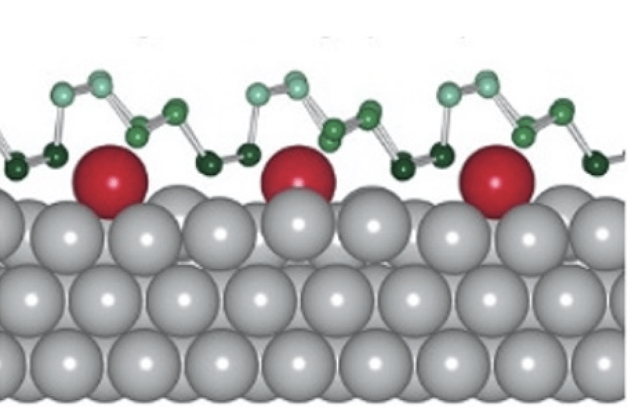
Properties of chiral molecule / metallic interfaces
Laboratoire: MPQ (Matériaux et Phénomènes Quantiques), Université Paris Cité & CNRSAdresse: Bâtiment Condorcet – 10 Rue A. Domon et L. Duquet – 75013 ParisDirecteur de stage/thèse: Amandine BellecTel: 0157276290e-mail: amandine.bellec@u-paris.fr Scientific...

Postdoc : Integrated Quantum Optoelectronics
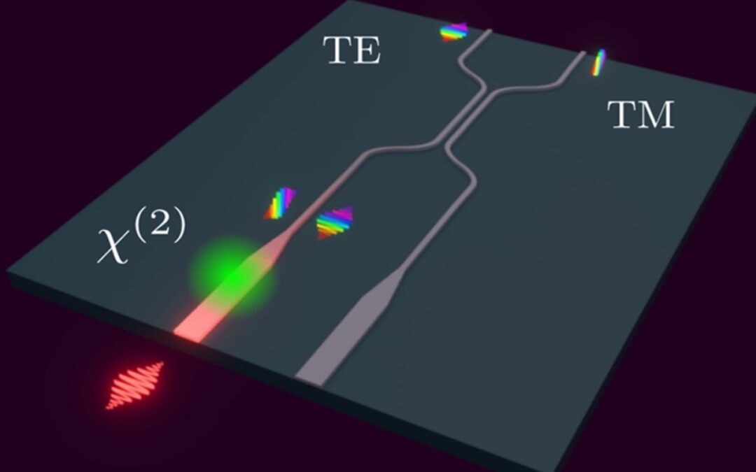
The Quantum Information and Technologies team is hiring a highly motivated postdoctoral researcher to work in the exciting field of nonlinear integrated quantum photonics. The successful candidate will work in a highly collaborative research environment, have access...

Postdoc: Experimental Quantum Optics
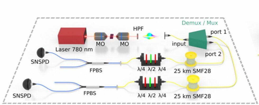
The Quantum Information and Technologies team is hiring a highly motivated postdoctoral researcher to work in the exciting field of integrated photonics for quantum information. The successful candidate will work in a highly collaborative research environment...
