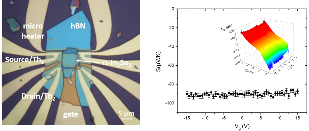
LEFT) Optical microscope image of a device based on α-In2Se3 . RIGHT) Measured Seebeck coefficient of α-In2Se3 as a function of the gate voltage. Inset: current-voltage characteristics of the device for different values of the gate voltage.
Laboratoire: MPQ (Matériaux et Phénomènes Quantiques), Université Paris Cité & CNRS
Adresse: Bâtiment Condorcet – 10 Rue A. Domon et L. Duquet – 75013 Paris
Directeur de stage/thèse: Maria Luisa Della Rocca
Tel: 0157277013
e-mail: maria-luisa.della-rocca@u-paris.fr
Scientific project:
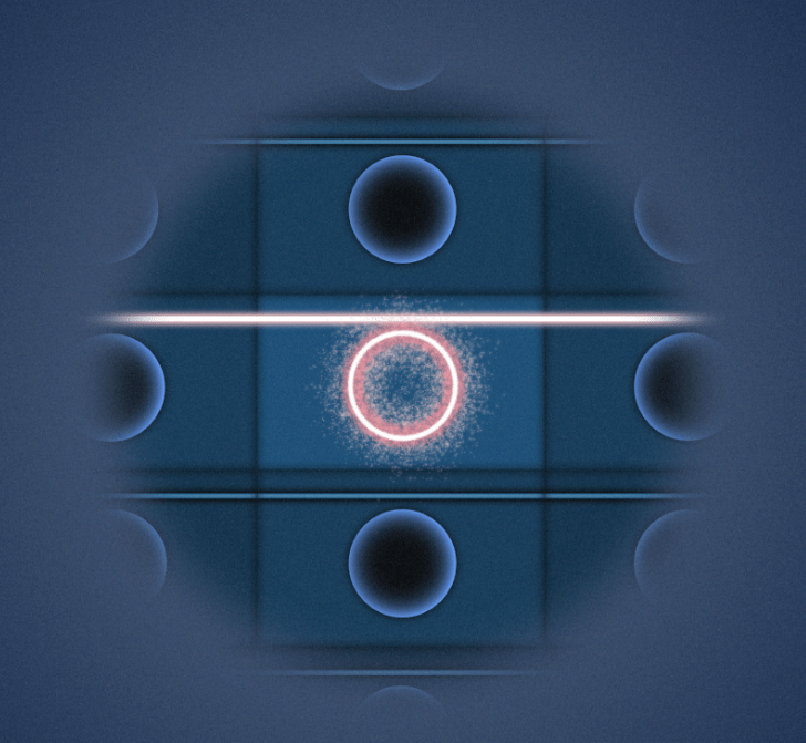
Recently bidimensional (2D) van der Waals (vdW) III−VI semiconductors have drawn intense attention due to their unique electronic properties [1]. Among these materials, In2Se3 in its most studied a and b phases, shows a great potential for a wide variety of applications in electronics, photonics and even thermoelectricity, due to its good mobility, excellent photoresponsivity, exotic ferroelectricity, and unique band structure [2-4]. In2Se3 possess an in- and out-of-plane ferroelectricity, which remains robust down to the monolayer limit. Moreover, very recently, 2H α-In2Se3 single crystals have also shown the occurrence of a 2D electron gas (2DEG) at their surface [5] (see Fig.), with high electron density (~1013 elec/cm2) even at room temperature, comparable to what achieved in AlGaN/GaN material systems. First-principles calculations based on the density functional theory and Boltzmann transport theory show that monolayered α-In2Se3 is also a great candidate for high-performance thermoelectric materials with the power factor PF and the figure of merit ZT as high as 0.02W/mK2 and 2.18 at room temperature [4].
In this context, the main goal of the internship is to go a step forward in the investigation of the thermoelectric properties of α-In2Se3 and the influence of the 2DEG formed at its surface on the electric and thermoelectric response. The student will fabricate α-In2Se3 based devices in a 4 contact configuration with a local gate for electric and thermoelectric investigation. The activity will cover sample fabrication in clean room (dry transfer of the 2D material, e-beam lithography, etching, metal deposition …) and electrical measurements in a multi-probe station as a function of the temperature. The team has a strong expertise in the investigation of charge and spin transport in 2D materials and in clean room micro and nano fabrication techniques. This expertise will be exploited in the project.
[2] Z. Yu et al. Nano Lett. 17, 5508 (2017)
[3] P. Hou et al., ACS Appl. Electron. Mater. 2, 140 (2020)
[4] T. Nian et al., Appl. Phys. Lett. 118, 033103 (2021)
[5] G. Kramer et al., https://doi.org/10.1021/acsnano.3c04186
Methods and techniques: micro‐fabrication in clean room, transport measurements
Possibility to go on with a PhD: YES
Envisaged fellowship: participation to the EDPIF competition and/or PhD funding in submitted project
À lire aussi

TUPHO, pour la production à grande échelle de circuits photoniques intégrés
Le projet TUPHO est une initiative qui veut combler le fossé entre innovation en amont et production à grande échelle dans l’industrie des circuits photoniques intégrés (PICs). Il est porté par Hamidreza Neshasteh et Ivan Favero, membres de l’équipe Light and...

Manipulating unconventional superconducting states via anisotropic strain
Laboratoire: MPQ (Matériaux et Phénomènes Quantiques), Université Paris Cité & CNRSAdress: Bâtiment Condorcet – 10 Rue A. Domon et L. Duquet – 75013 ParisInternship/PhD supervisor: Yann GallaisTel: 0157276989e-mail: yann.gallais@u-paris.fr Scientific project:...

Towards light control of van der Waals magnets
Laboratoire: MPQ (Matériaux et Phénomènes Quantiques), Université Paris Cité & CNRS Adress: Bâtiment Condorcet – 10 Rue A. Domon et L. Duquet – 75013 Paris Internship/PhD supervisor: Niloufar Nilforoushan and Yann Gallais Tel: 0157276223 e-mail:...

Séminaires
2025-2026 MPQ general seminar series organized by Niloufar Nilforoushan and Valentin Cambier Prof. Sebastian Loth — Institute for Functional Matter and Quantum Technologies, University of Stuttgart, Germany Title: Coming soon Jan. 16, 2026 at 11:00 am — Salle Luc...
